As copper connections on PCBs approach the limit of their bandwidth capabilities due to constraints in space, noise, and power, electronics manufacturers are looking for innovative technologies to power the next generation of interconnects that can offer the bandwidth required by upcoming AI technologies, processors and quantum computing applications. To overcome copper traces' limitations, photonics in hybrid electro-optical printed circuit boards (HEOPCB) will likely be adopted in the next few years.
HEOPCBs are made by combining electrical and optical components into a single unit, but manufacturing this kind of board can be challenging with the current processes. Three-dimensional (or "additive") printing technology provides a way to manufacture this new type of board and allows for creating smaller, lighter, and more intricate designs than possible with traditional PCB manufacturing methods, with lower power consumption and less water pollution. HEOPCBs also offer improved resistance to electromagnetic interference (EMI) and can be used to create circuits with a higher component density.
Where HEOPCBs come into play
Chips are always getting faster, and the need for computing power seems endless for applications like Artificial Intelligence and Machine Learning. But with computing power comes the need to move the data at even higher speeds. Hence high-bandwidth applications are the future of electronics.
Faster chips will require larger bandwidth communication channels to achieve the throughput they were designed for. But increasing throughput on the same number of pins does not scale since higher frequencies will yield additional noise and heat, and increasing the number of pins (connectors) will increase the cost and size of the electronics. A breakdown of the reasons why copper traces don’t seem to scale anymore is shown below:
- Capacitance/resistance of copper wire won't allow faster transmissions due to limitations on rise and fall times
- Signal switching at higher frequencies creates higher EMI
- Faster switching will create greater power dissipation on the lines (heat)
- Increasing throughput by adding more pins to the chips means:
- Larger and more expensive packages
- More metal routing inside the chip and a lower yield
- A larger area is required on the PCB for trace fan-out
- Higher complexity for designers
- Copper paths are still affected by Electromagnetic Interference (EMI)
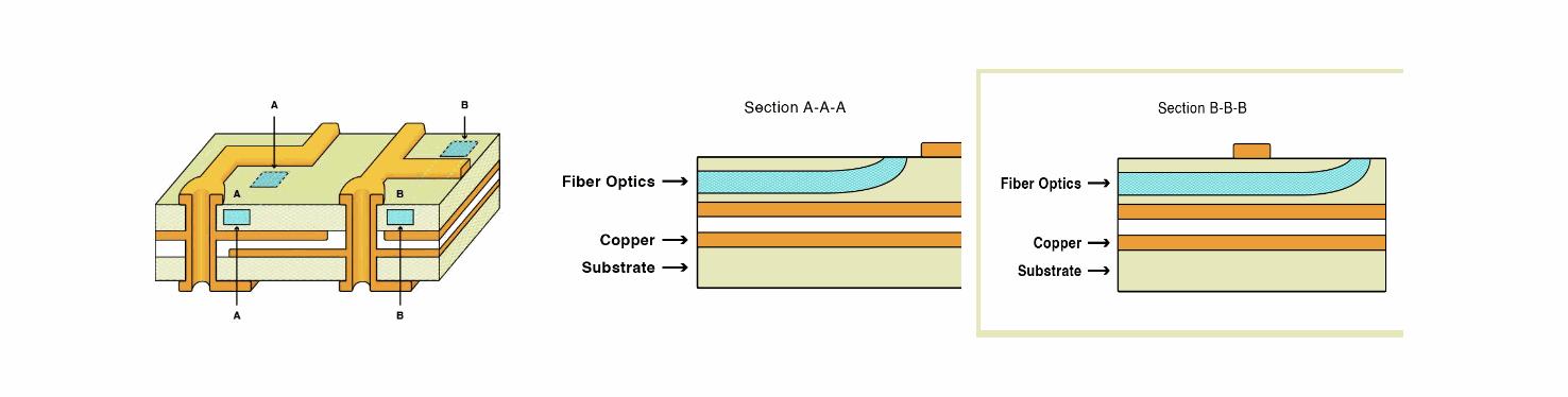
Hybrid electro-optical printed circuit boards overcome these problems by allowing high-bandwidth transmission lines to be implemented using fiber optics, while lower frequency signals use copper. They offer a unique way to improve the efficiency and speed of connections. 3D printing electro-optical waveguides onto a traditional printed circuit board will make it possible to create a board that can carry electrical and optical signals in one package.
This has several advantages:
Improved performance
Because the electrical and optical components are integrated onto one board, the designer has the freedom to use photonic-enabled or all-electric chips as needed in the same design. While all-electric chips use copper, capping their bandwidth to about 40Gbps per line, Photonic-enabled chips can now take advantage of their massive bandwidth capability by using chip-to-chip interconnects based on the optical fiber embedded inside the board. This means that chip-to-chip connections can run at 100Tbps or more, based on the fiber configuration. This is a huge gain!
Smaller size
Optical waveguides are smaller than typical copper traces, usually around 50um wide. They can easily carry 1000X the amount of data as copper. It would allow the designer to reduce the board size by replacing several copper traces with a single optical fiber.
In the same direction, you don't need separate electrical and optical components boards - they can all be integrated onto one substrate.
Additionally, 3D printing can create complex electro-optical circuits with very small feature sizes. This allows for further increases in density and speeds up the flow of information.
Better energy efficiency
Photonic systems use photons to carry information through optic fibers, while electrical systems use electrons that travel on conductors, usually metal. Traditional electronics create heat through the interaction between the electrons and the conductor. When the heat goes uncontrolled, the performance of the systems gets hindered because this interaction increases, generating additional noise. That is why data centers spend millions of dollars cooling their servers. With the addition of optical components and connections, the amount of heat generated by the system will be considerably lower, improving the device's performance, and lowering the AC bill.
Immunity to EMI
EMI (electromagnetic interference) happens due to the electromagnetic (EM) fields created around a wire when the current fluctuates, which is quite common in most electronic applications. The EM fields created on a wire will travel through different materials (including air) and eventually induce a current in a different nearby conductor. After all, this is the principle radios work on. The issue is that the EM fields can induce a current in the wrong wire in the circuit, creating interference in the data that the receiving wire is transmitting. The effect of EMI on wires is so common that most electronic designs account for it by using encodings that allow the recovery of data when it is slightly noisy, and very careful routing of the copper wires. Too much interference on a single wire and the communication channel becomes too noisy to be useful.
Electro-optical waveguides are not affected by electromagnetic interference like copper. They don’t produce electromagnetic fields around the fiber, not even when switching at high frequencies, and surrounding EM fields won’t affect it, so they can be used to transmit signals without fear of distortion, even when pushing for the fastest transfer rates.
Potential drawbacks to using HEOPCBs
While electro-optical printed circuit boards offer many potential benefits, there are also some potential drawbacks. 3D printing HEOPCBs is a killer app. However, the challenge is that electro-optical circuits are difficult to 3D print, requiring very precise layer thicknesses and alignment. Additionally, electro-optical materials can be expensive and may not be readily available.
HEOPCBs can be more difficult to manufacture than traditional PCBs due to the need for specialized materials and equipment, but further than that, the technology hasn't gone through a standardization process. This makes it so that some chip manufacturers will require the fibers to be connected on the side of the chip, some will need a connection at the top, and a few will agree to connect to the fibers under the chip. Luckily for the technology, it's 3D printing nature would allow plenty of flexibility when it comes to adapting to each of the manufacturer's need.
Finally, electro-optical printed circuit boards are still a relatively new technology, so there is potential for unexpected issues to arise during printing, fabrication, or use.
Despite these challenges, electro-optical printed circuit boards hold great promise for various applications. With continued development, researchers and engineers will overcome these potential pitfalls, and over the next five years, electro-optical printed circuit boards will see increased usage.
Future of HEOPCBs: 3D printing
Copper on printed circuit boards is starting to hit its limitations for performance and the number of traces that can be fit on a board. Photonics is the next generation ‘substance’ that will allow boards to meet the ever-increasing demand for smaller, faster circuits that use less energy.
As technology advances, it's important to keep up with what is possible. And one of the most promising applications for photonics is 3D printed, electro-optical circuit boards. These circuit boards will soon power tomorrow's quantum computing apps based on artificial intelligence and machine learning.
BotFactory is leading the research to make 3D-printed electro-optical printed circuit boards a reality. This technology can potentially change how we build and use electronics completely. With photonics, we'll be able to create printed circuit boards with increased complexity and higher performance but also much smaller components that use a fraction of the electricity that today’s boards consume. This will allow us to build even more powerful computers and gadgets in the long-term future.
It's exciting to think about all the new ideas that photonics will help make a reality for the future of computing. We can't wait to see what amazing things will be built when this technology becomes mainstream.
BotFactory Efforts
Today, BotFactory is researching ways to create hybrid opto-electrical interconnects.
Many photonics efforts are focusing on in-silicon communication, which is adding optical connections to chips. However, there is also a strong need for point-to-point connections to be made with single fiber optic cables.
If the connections become more complex (they always do), printed hybrid opto-electrical PCBs will play an important role. Today we are actively researching methods for embedding fiber optics to connect components as part of our additive 3D printed circuit board technology. The goal is that soon, this technology will be added to our line of desktop 3d circuit board printers.
About BotFactory
BotFactory is the leader in desktop additive manufacturing of electronics, offering machines capable of printing multi-layer PCBs, dispensing paste, and picking and placing components in a single system. BotFactory's solutions enable on-site and same-day manufacturing for R&D teams worldwide.