Think you need a lab to prototype electronics?
We've proven you don't.
Although Botfactory's products are created with an R&D-lab setting in mind, they have provided fortuitous value during the recent events that have stranded electrical engineers working from home.
With the various departments of every company dispersed at their houses, the known delays and limitations associated with PCB prototyping have gotten worse.
- Getting a budget approval and coordinating purchasing becomes an email marathon (or a Zoom party)
- Finding a board manufacturer unaffected by prohibitive delivery times and MOQs -due to the much larger backlogged orders- is a hurdle (especially when both fabrication and assembly [PCB/A] are required)
- Shipping the boards to all the necessary team members requires further processing and an additional shipping step
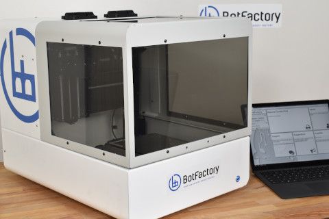
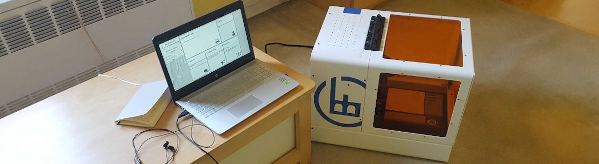
Botfactory, since its birth in 2013 in NY, has been led by the premise that bringing your electronics ideas to life should not require an outside service, but should be done with an in-house product, on your desk. Taking that a step further and providing the ability to create PCBs at home, is a natural consequence of our philosophy. This ability has become invaluable during the COVID-19 pandemic.
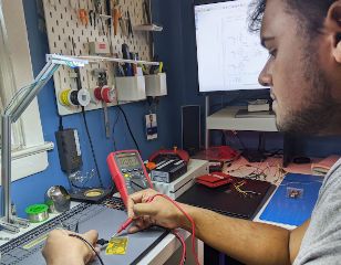
When Governor Cuomo announced the "New York State on PAUSE" executive order, our team was quick to take what mattered the most out of the office: the BotFactory SV2s used internally. Being a tech firm, R&D is one of our most valuable assets and we knew we could not afford the imminent productivity loss. The decision paid off pretty quickly.
With many of the PCB/A manufacturers either closed or overloaded by the bigger customers, getting smaller/prototype batches became even slower and harder than usual. Giving our engineers the ability to continue developing, testing, and iterating circuit boards while at home allowed us to both mitigate the effects of the "PAUSE" on R&D and have a proper test run of what working from home can look like, especially for the scientific and technical services.
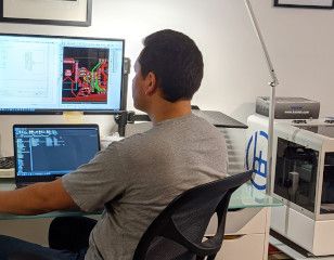
Circuit Design
Circuit Review
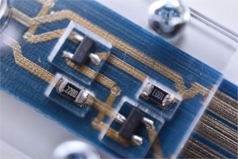
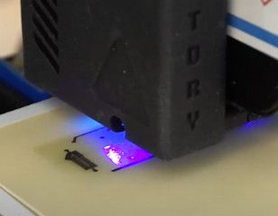
Circuit Build
Our desktop circuit "factories" have been cranking out electronics in the most innovative companies, labs, and universities in more than 40 countries around the globe; now, we are adding residential addresses to the list.
No matter where you work from, we keep on pushing the boundaries of what distributed, on-demand, at-place electronic PCB/A should look like, allowing seamless collaboration with your team, whether they are a cubicle, a town, or a continent away.